") NCP51705主要特性_內(nèi)部框圖以及應(yīng)用電路
NCP51705主要特性_內(nèi)部框圖以及應(yīng)用電路

On Semi公司的NCP51705驅(qū)動(dòng)器是設(shè)計(jì)用來(lái)驅(qū)動(dòng)SiC MOSFET晶體管,為了得到盡可能低導(dǎo)通損耗,驅(qū)動(dòng)器能驅(qū)動(dòng)SiC MOSFET器件的最大可允許柵極電壓,源電流和沉電流為6A,并提供重要的保護(hù)功能如基本電源的欠壓鎖住監(jiān)視和基于驅(qū)動(dòng)電路的結(jié)溫的熱關(guān)斷,主要用在驅(qū)動(dòng)SiC MOSFET晶體管,工業(yè)逆變器,馬達(dá)驅(qū)動(dòng)和PFC,AC疍C轉(zhuǎn)換器和DC/DC轉(zhuǎn)換器.本文介紹了NCP51705主要特性,內(nèi)部框圖,低邊開(kāi)關(guān)配置圖和應(yīng)用電路,以及NCP51705 Mini 評(píng)估板和NCP51705 Mini SMD評(píng)估板主要特性,電路圖,材料清單和PCB設(shè)計(jì)圖.
The NCP51705 driver is designed to primarily drive SiC MOSFETtransistors. To achieve the lowest possible conduction losses, thedriver is capable to deliver the maximum allowable gate voltage to theSiC MOSFET device. By providing high peak current during turn?onand turn?off, switching losses are also minimized. For improvedreliability, dV/dt immunity and even faster turn?off, the NCP51705can utilize its on?board charge pump to generate a user selectablenegative voltage rail.
For full compatibility and to minimize the complexity of the biassolution in isolated gate drive applications the NCP51705 alsoprovides an externally accessible 5 V rail to power the secondary sideof digital or high speed opto isolators.
The NCP51705 offers important protection functions such asunder?voltage lockout monitoring for the bias power and thermalshutdown based on the junction temperature of the driver circuit.
NCP51705主要特性:
? High Peak Output Current with Split Output Stages to allowindependent Turn?ON/Turn?OFF Adjustment;
? Source Capability: 6 A
? Sink Capability: 6 A
? Extended Positive Voltage Rating for Efficient SiC MOSFETOperation during the Conduction Period
? User?adjustable Built?in Negative Charge Pump for Fast Turn?offand Robust dV/dt Immunity
? Accessible 5 V Reference/Bias Rail for Digital Oscillator Supply
? Adjustable Under?Voltage Lockout
? Desaturation Function
? Thermal Shutdown Function (TSD)
? Small & Low Parasitic Inductance QFN24 Package
NCP51705典型應(yīng)用:
? Driving SiC MOSFET
? Industrial Inverters, Motor Drivers
? PFC, AC to DC and DC to DC Converters

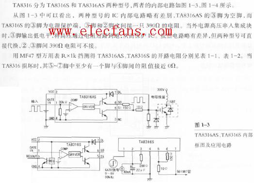
圖1.NCP51705內(nèi)部框圖

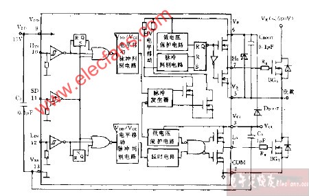
圖2.NCP51705低邊開(kāi)關(guān)配置圖

圖3.NCP51705典型應(yīng)用電路圖

圖4. NCP51705半橋柵極驅(qū)動(dòng)電路圖
NCP51705 Mini 評(píng)估板
This document describes the use and applications for theNCP51705 SiC driver mini EVB. The EVB is designed ona four layer PCB and includes the NCP51705 driver and all the necessary drive circuitry. The EVB also includes anon?board digital isolator and the ability to solder anyMOSFET or SiC MOSFET in a T0247 high voltagepackage. The EVB does not include a power stage and isgeneric from the point of view that it is not dedicated to anyparticular topology. It can be used in any low?side orhigh?side power switching application. For bridgeconfigurations two or more of these EVBs can be configuredin a totem pole type drive configuration. The EVB can beconsidered as an isolator+driver+T0247 discrete module.
圖5.評(píng)估板NCP51705 EVB(35 mm x 15 mm x 5 mm)外形圖

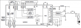
圖6.評(píng)估板NCP51705 EVB電路圖
評(píng)估板NCP51705 EVB材料清單:


圖7.評(píng)估板NCP51705 EVB頂層裝配圖

圖8.評(píng)估板NCP51705 EVB底層裝配圖

圖9.評(píng)估板NCP51705 EVB頂層圖

圖10.評(píng)估板NCP51705 EVB層2圖

圖11.評(píng)估板NCP51705 EVB層3圖

圖12.評(píng)估板NCP51705 EVB底層圖
NCP51705 Mini SMD評(píng)估板
This document describes the use and applications for the NCP51705SiC driver mini SMD EVB. The EVB is designed on a four layer PCBand includes the NCP51705 driver and all the necessary drivecircuitry. The EVB also includes an on?board digital isolator and the ability to solder any MOSFET or SiC MOSFET in a TO?247 highvoltage package. The EVB does not include a power stage and isgeneric from the point of view that it is not dedicated to any particulartopology. It can be used in any low?side or high?side power switchingapplication. For bridge configurations two or more of these EVBs canbe configured in a totem pole type drive configuration. The EVB canbe considered as an isolator+driver+TO?247 discrete module.
圖13.NCP51705 Mini SMD評(píng)估板外形圖(1)
圖14.NCP51705 Mini SMD評(píng)估板頂層和底層圖

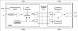
圖15.NCP51705 Mini SMD評(píng)估板簡(jiǎn)化框圖

圖16.NCP51705 Mini SMD評(píng)估板電路圖
NCP51705 Mini SMD評(píng)估板材料清單:


圖17.NCP51705 Mini SMD評(píng)估板PCB頂/底層裝配圖

圖18.NCP51705 Mini SMD評(píng)估板PCBINNER_1/INNER_2層布局圖

圖19.NCP51705 SiC EVB PCB打孔圖

圖20.NCP51705 SiC EVB未安裝時(shí)PCB的測(cè)試配置圖
-
變換器
+關(guān)注
關(guān)注
17文章
2152瀏覽量
111864 -
DC/DC變換器
+關(guān)注
關(guān)注
0文章
4瀏覽量
5380
發(fā)布評(píng)論請(qǐng)先 登錄
開(kāi)關(guān)穩(wěn)壓器NCP3065資料推薦
電源控制芯片NCP1239F相關(guān)資料下載
電源管理芯片NCP1294相關(guān)資料分享
LED驅(qū)動(dòng)器NCP5602相關(guān)資料分享
超小型RGBLED驅(qū)動(dòng)電路NCP5623資料推薦
POEPD以太網(wǎng)供電用電設(shè)備控制器NCP1081資料推薦
AD8452主要特性_框圖以及應(yīng)用電路
ISO224主要特性以及應(yīng)用電路
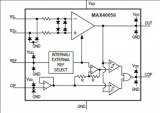
MAX40056主要特性以及應(yīng)用電路
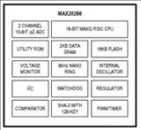
MAX28200優(yōu)勢(shì)特性以及基本應(yīng)用電路
MAX86150的優(yōu)勢(shì)特性以及典型應(yīng)用電路圖
NCP51705 SiC MOSFET驅(qū)動(dòng)器 低側(cè) 單個(gè)6A高速
NCP1611控制器的主要特性及應(yīng)用通用電路


 工商網(wǎng)監(jiān)
評(píng)論